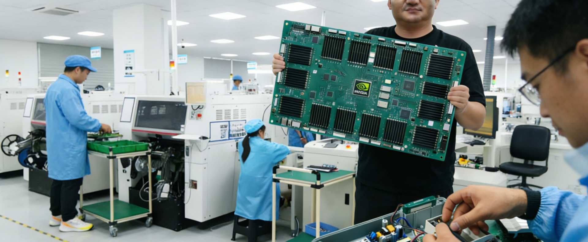
PCB manufacturing team and precision electronics assembly workshopPrecision PCB production and assemblyPrecision PCB production and assembly

PCB/PCBAManufacturing &Assembly

One-stop solution from prototyping to mass production, specializing in multi-layer, high-complexity PCB and PCBA for military, medical, automotive and industrial applications.

Why Choose ShwayPCB

Fast Turnaround

48h standard prototype, 24h urgent delivery for high-complexity PCBs

High Precision

01005 components, 0.2mm BGA, 2mil/2mil line width/spacing, ±3Ω impedance control

Strict Quality

99.8% yield rate, IPC-A-610 Class 3, ISO 13485/IATF 16949 certified

One-Stop Service

From design to prototyping, assembly, testing and global delivery

High Complexity

2-98 layers PCB (focus on 8-64 layers), blind/buried via, thick copper (10-20oz)

Global Service

1000+ global customers, 80% repeat purchase rate, confidential NDA agreement

Competitive Pricing

Factory-direct pricing with no middleman markup, transparent cost breakdown, volume discounts

Technical Support

24/7 engineering support, DFM analysis free of charge, lifetime technical consultation

Core Services

Multilayer PCB Prototype

  • Layers: 2-98 Layers (Focus on 8-64 Layers)
  • Line Width/Spacing: 2mil/2mil
  • Hole Size: 0.1mm Microvia
  • Impedance Control: ±3Ω
  • Substrate: FR4 (High-Tg), Rogers, Taconic
  • Turnaround: 48h (Standard), 24h (Urgent)
  • Support blind/buried via, thick copper (10-20oz), step slot

High-precision PCBA Assembly

  • Assembly Type: SMT, DIP, BGA/QFP/CSP Soldering
  • Component Size: 01005 Package (Smallest)
  • Inspection: AOI, X-Ray, ICT, FCT Testing
  • Material Supply: Customer Supplied / Full Turnkey
  • Volume: 1-5000 Sets (Prototype Low-Volume)
  • ESD anti-static workshop, IPC-A-610 Class 3 standard

PCB Design Layout

  • Design Scope: 2-64 layers PCB design
  • Design Optimization: DFM/DFA, Impedance Matching, SI Analysis
  • Application: Medical, Automotive, Military, Industrial Control
  • Delivery: Gerber, BOM, Schematic, Design Spec
  • Compliance: IPC-2221/2222, RoHS/REACH

BGA Rework Service

  • Rework Type: BGA Desoldering, Resoldering, Replacement
  • Precision Control: High-precision Hot Air Station
  • Applicable Components: ≥0.2mm Pitch BGA/QFP/CSP
  • Inspection: X-Ray Before/After Rework
  • Protection: Preheating, Anti-static Operation

PCBA Reverse Engineering

  • Scope: Schematic Recovery, Layout Extraction, BOM Organization
  • Capability: Up to 32 layers PCB, HDI Boards
  • Delivery: Gerber, Schematic, BOM, Assembly Drawings
  • Quality: Circuit Function Consistency Verification
  • Compliance: Legal Authorization, IP Protection

One-stop Solution

  • Design Support: DFM/DFA Audit, Impedance Optimization
  • Material Sourcing: Global Genuine Components
  • Testing: Reliability, Aging, Environmental Testing
  • Compliance: ISO 13485, IATF 16949
  • Logistics: Global Delivery with Insurance

High-Frequency & High-Speed Solutions

  • Frequency Range: DC-60GHz High-Frequency Design
  • Material: Rogers, Taconic, Isola High-Speed Material
  • Impedance: ±2Ω Ultra-Precision Impedance Control
  • SI/PI Analysis: Signal/Power Integrity Simulation
  • Application: 5G/6G, Radar, High-Speed Server
  • Process: Microvia, Air Gap, Laser Drilling

OEM & ODM Solutions

  • OEM Service: Custom Production as Per Customer Design
  • ODM Service: Full Design & Manufacturing Turnkey
  • Product Development: From Concept to Mass Production
  • Supply Chain: One-Stop Material Sourcing & Management
  • Quality: Batch Consistency & Traceability Guarantee
  • Flexibility: Small MOQ & Fast Customization Support

Box Build Electronics Assembly

  • Assembly Scope: Complete Product Integration & Testing
  • Process: PCBA + Mechanical Assembly + Cable Harness
  • Testing: Functional Testing, Burn-in Testing, Aging Test
  • Packaging: Custom Packaging & Labeling as Per Requirement
  • Compliance: CE/FCC/UL Certification Support
  • Logistics: Global Delivery & After-Sales Support

Detailed Technical Parameters

Comprehensive technical specifications to meet various application needs from consumer electronics to aerospace

ProjectStandard capabilitiesAdvanced abilitiesRemark
Number of layers2-16 layers18-98 layersSupports blind and buried vias, and arbitrary layer interconnection.
Board thickness range0.2-3.2mm0.1-12.0mmTolerance: ±10%
Minimum line width/spacing3/3mil (0.075mm)2/2mil (0.05mm)Direct laser imaging
Minimum aperture0.2mm mechanical drilling0.1mm laser micro-holeAspect ratio: 20:1
Impedance control±10%±3ΩSingle-ended/differential impedance
Surface treatmentLead-containing/lead-free solder plating, immersion goldImmersion silver, immersion tin, OSP, electroplated hard goldRoHS compliant
Copper thickness range0.5-2.0oz3.0-12.0ozThick copper plate
Warpage control≤0.75%≤0.3%High-precision pressing process